
The most indispensable component in electronic circuits and supplies is the Printed Circuit Board (PCB). It is likewise conceivable to construct an electronic circuit with breadboards and zero boards. However, the technique is a low level and less productive one wherein the designing circuit is inclined to harm. The designing includes a problematic procedure of putting the segments of the circuit.
However, the creation of the printed circuit boards that supports physical, electronic components and their wiring through the surface-mounted copper tracks are exceptionally noteworthy. We can see at any rate one Printed Circuit Board Design in any electronic contraptions running from mobile phones to PCs.
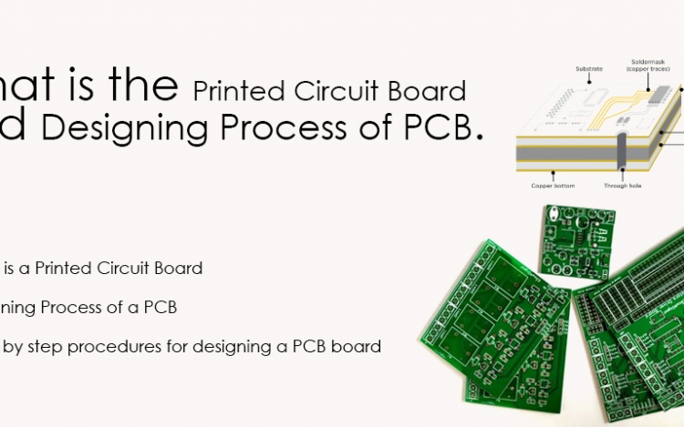
What is a Printed Circuit Board?
Electronic circuits in engineering and industry regularly manufacture using printed circuit boards (PCBs). These boards made of excellent materials that don’t direct electricity, for example, fiber and glass. Circuits structured on boards with copper tracks rather than wires for conduction electricity between electronic segments.
The electronic parts are fixed in their situations by boring openings on the Board, putting the components and afterward binding them in suitable positions with the goal that the copper tracks and parts together structure a circuit. The printed circuit boards used in every electronic item, for example, automotive, remote gadgets, Robotic applications, and so forth.
They offer brisk working, get to, control, observing, and exact and precise outcomes when contrasted with other wiring techniques based gadgets.
Designing Process of a PCB
Rely upon printed circuit board manufacturer; there are various ways accessible for structuring PCBs. This circuit board configuration can produce as mass using a few machines in flexible printed circuits manufacture ventures, including penetrating, punching, plating, and last creation forms that perform through profoundly computerized machines.
Laser boring with CNC machines, programmed plating machines, strip carving machines, and utilization of optical examination types of gear, flying test analyzers for electrical testing of printed circuit load up procedure bring about top-notch PCBs (with a more prominent generation yield).
Step- by step procedures for designing a PCB board
Design the PCB circuit with a Software
Draw the schematic circuit chart with the Printed Circuit Board Design software, for example, CAD programming, Eagle, and Multisim software. This kind of PCB structure software contains a library of segments that can be utilized to fabricate the circuit.
It is likewise conceivable to change the circuit configuration’s position and afterward to adjust as indicated by your accommodation and prerequisite. Here we have chosen Eagle programming to structure the circuit, and its system is as per the following:
Film Generation
The film is created from the concluded circuit board chart of the PCB design programming, which is sent to the assembling unit where the negative picture or cover is printed out on a plastic sheet.
Select Raw Material
The central part of the printed circuit board is made with an unbreakable glass or fiberglass having copper foil reinforced unto one or both sides of the Board.
In this way, the Printed Circuit Board produced using durable paper phenolic with a reinforced copper foil are more affordable and are regularly utilized in family unit electrical gadgets.
Preparing Drill Holes
Machines and carbide drills are utilized to put gaps on the printed circuit board. There are two kinds of machines accessible to drill the flexible printed circuits; they incorporate hand machines and CNC machines.
The hand machines require human mediation or exertion to penetrate the gaps, while CNC machines are PC put together machines that work-based concerning on the machine timetables or projects that run both programmed just as physically.
The drilled example is put away in the PC like boring tool sizes, several gaps per Board, penetrated stack, drilled time per load, and so on. The PCB sheets put into the CNC machine, and the holes are drilled to place printed circuit board parts.
Apply Image
The printed circuit format can imprint in various manners on PCBs like a manual pen, dry exchanges, pen plotters, and printers. The laser printers are a superior method to print the formats on printed circuit sheets. The accompanying advances are utilized to reproduce the PCB design through a laser printer:
Stripping and Etching
This procedure includes expelling the unwired copper on the PCBs by utilizing various kinds of synthetic concoctions like ferric chloride, ammonium persulfate, and so forth. Make the dissolvable by blending 1% of sodium hydroxide and 10 grams of sodium hydroxide pellets to one liter of water and mix it until everything is broken down.
Next, the PCB is put on a substance bowl and tidied up with a brush. During this procedure, if the PCB is as yet oily, because of applied sunflower or seed oil, the creating process may take around one moment.
Testing
After completing the assembling procedure of the Printed Circuit Board, the Board experiences a testing procedure to check whether the PCB is working appropriately. These days numerous programmed testing types of gear are accessible for the high volume testing of the PCBs.